FPGAVerilog 编码实现:与非门 | 或非门 | 异或门 | NAND/NOR/XOR 行为验证
Posted 柠檬叶子C
tags:
篇首语:本文由小常识网(cha138.com)小编为大家整理,主要介绍了FPGAVerilog 编码实现:与非门 | 或非门 | 异或门 | NAND/NOR/XOR 行为验证相关的知识,希望对你有一定的参考价值。

写在前面:本章主要内容为了解和确认 NAND/NOR/XOR 门的行为,并使用Verilog实现,生成输入信号后通过模拟,验证每个门的操作,并使用 FPGA 来验证 Verilog 实现的电路的行为。
本章目录:
0x03 4-input AOI(AND OR Inverter) gate
Ⅰ. 前置知识
0x00 与非门(NAND)
如果所有输入均为High (1),则输出为Low (0),在其他情况下,将产生High (1) 输出。
- NAND 是 AND 运算符的否定结果
布尔表达式中以 "负乘法" 形式表现:


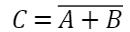
0x01 或非门(NOR)
如果所有输入均为 Low (0),则输出为 High(1),其中一个输入为高 (1) 则产生低功率 (0)。
- NOR 是 OR 运算符的否定结果
布尔表达式中以 "否定合" 形式表现:

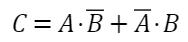
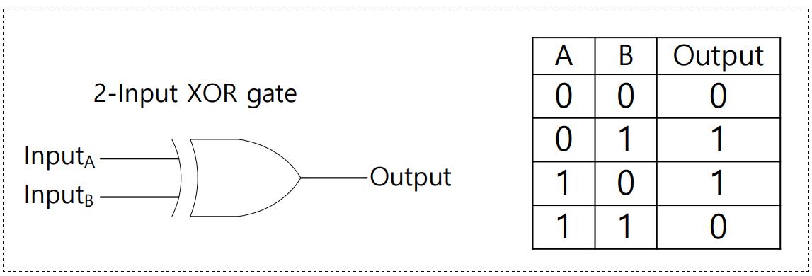
0x02 异或门(XOR)
如果 两个值不相同,则异或结果为1。如果 两个值相同,异或结果为0。
Ⅱ. 练习(Assignment)
0x00 4-input NAND gate
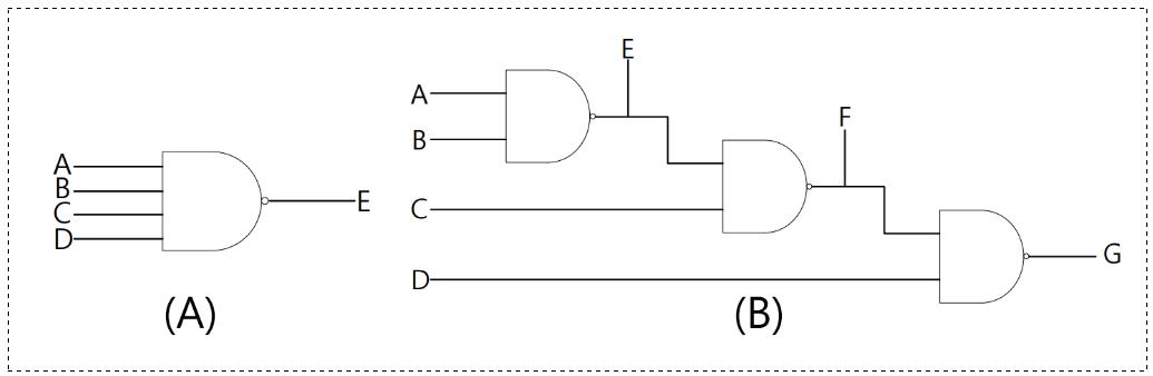
比较 AB 的布尔表达式,完成 A 和 B 的 Verilog 代码,通过 Simulation 结果进行比较。
💬 Design source:
`timescale 1ns / 1ps

module input_4_NAND(
    // Input the var
    input a, b, c, d,
    // Output the var
    output e, f, g
    );

// NAND = NOT + AND
assign e = ~(a & b);    // a and b then inv
assign f = ~(e & c);    // e and c then inv
assign g = ~(f & d);    // f and d then inv

endmodule
💬 Simulation:
`timescale 1ns / 1ps

module input_4_NAND_tb;
reg aa, bb, cc, dd;
wire e, f, g;

input_4_NAND u_input_4_NAND (
    .a(aa),
    .b(bb),
    .c(cc),
    .d(dd),
    .e(e),
    .f(f),
    .g(g)
    );

initial aa = 1'b0;
initial bb = 1'b0;
initial cc = 1'b0;
initial dd = 1'b0;

always aa = #100 ~aa;
always bb = #200 ~bb;
always cc = #400 ~cc;
always dd = #800 ~dd;

initial begin
    #1600
    $finish;
end

endmodule
🚩 运行结果如下:

💡 解读:在 assign 语句中,用取反运算符 ~ 和或运算符 | 实现了 4 个输入取反或运算,并将结果分别赋值给输出变量 e, f, g。
0x01 4-input NOR gate

比较 AB 的布尔表达式,完成 A 和 B 的 Verilog 代码,通过 Simulation 结果进行比较。
💬 Design source:
`timescale 1ns / 1ps

module input_4_NOR(
    /* Input the var */
    input a, b, c, d,
    /* Output the var */
    output e, f, g
    );

/* NOR = NOT + OR */
assign e = ~(a | b);
assign f = ~(e | c);
assign g = ~(f | d);

endmodule
💬 Testbench:
`timescale 1ns / 1ps

// input_4_NOR_tb

module input_4_NOR_tb;
// input
reg aa, bb, cc, dd;
// output
wire e, f, g;

input_4_NOR u_input_4_NOR (
    .a(aa),
    .b(bb),
    .c(cc),
    .d(dd),

    .e(e),
    .f(f),
    .g(g)
    );

initial aa = 1'b0;
initial bb = 1'b0;
initial cc = 1'b0;
initial dd = 1'b0;

always aa = #100 ~aa;
always bb = #200 ~bb;
always cc = #400 ~cc;
always dd = #800 ~dd;

initial begin
    #1600
    $finish;
end

endmodule
🚩 运行结果如下:

0x02 4-input XOR gate
比较 AB 的布尔表达式,完成 A 和 B 的 Verilog 代码,通过 Simulation 结果进行比较。

💬 Design source:
`timescale 1ns / 1ps

module input_4_XOR(
    /* Input the var */
    input a, b, c, d,
    /* Output the var */
    output e, f, g
);

/* XOR */
assign e = a ^ b;
assign f = e ^ c;
assign g = f ^ d;

endmodule
💬 Testbench:
`timescale 1ns / 1ps

module input_4_XOR_tb;
// input
reg aa, bb, cc, dd;
// output
wire e, f, g;

input_4_XOR u_input_4_XOR (
    .a(aa),
    .b(bb),
    .c(cc),
    .d(dd),

    .e(e),
    .f(f),
    .g(g)
    );

initial aa = 1'b0;
initial bb = 1'b0;
initial cc = 1'b0;
initial dd = 1'b0;

always aa = #100 ~aa;
always bb = #200 ~bb;
always cc = #400 ~cc;
always dd = #800 ~dd;

initial begin
    #1600
    $finish;
end

endmodule
🚩 运行结果如下:

0x03 4-input AOI(AND OR Inverter) gate
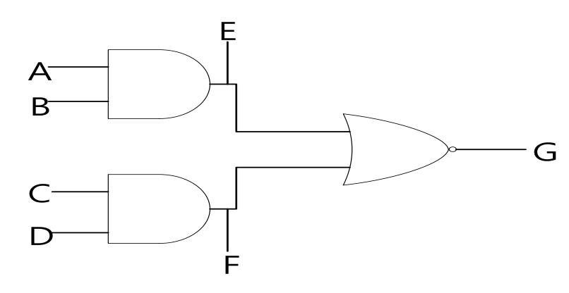
💬 Design source:
`timescale 1ns / 1ps
module inpu_4_AOI (
/* Input the var */
input a, b, c, d,
/* Output the var */
output e, f, g
);
/* AOI */
assign e = a & b;
assign f = e & c;
assign g = ~(e | f);
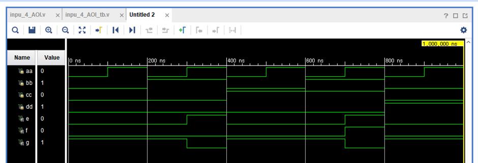
endmodule💬 Testbench:
`timescale 1ns / 1ps

module inpu_4_AOI_tb;
// input
reg aa, bb, cc, dd;
// output
wire e, f, g;

inpu_4_AOI u_inpu_4_AOI (
    .a(aa),
    .b(bb),
    .c(cc),
    .d(dd),

    .e(e),
    .f(f),
    .g(g)
    );

initial aa = 1'b0;
initial bb = 1'b0;
initial cc = 1'b0;
initial dd = 1'b0;

always aa = #100 ~aa;
always bb = #200 ~bb;
always cc = #400 ~cc;
always dd = #800 ~dd;

initial begin
    #1600
    $finish;
end

endmodule
🚩 运行结果如下:

📌 [ 笔者 ]   王亦优
📃 [ 更新 ]   2022.9.20
❌ [ 勘误 ]   /* 暂无 */
📜 [ 声明 ]   由于作者水平有限,本文有错误和不准确之处在所难免,
本人也很想知道这些错误,恳望读者批评指正!| 📜 参考资料 Introduction to Logic and Computer Design, Alan Marcovitz, McGrawHill, 2008 Microsoft. MSDN(Microsoft Developer Network)[EB/OL]. []. . 百度百科[EB/OL]. []. https://baike.baidu.com/. |
以上是关于FPGAVerilog 编码实现:与非门 | 或非门 | 异或门 | NAND/NOR/XOR 行为验证的主要内容,如果未能解决你的问题,请参考以下文章