PCM1863应用笔记
Posted NiceBT
tags:
篇首语:本文由小常识网(cha138.com)小编为大家整理,主要介绍了PCM1863应用笔记相关的知识,希望对你有一定的参考价值。
1. 配置需求
- 时钟输入:SCKI(24.576MHz)
- 模拟输入:VINL2(Stereo left channel),VINR2(Stereo right channel)
- LRCK:96KHz
- BCK:6.14MHz

2. 配置通信接口
In software SPI/I2C mode, a PCM186x software programmable device can use its on-chip crystal oscillator, if a CMOS clock source is not available.
通信口选择I2C:
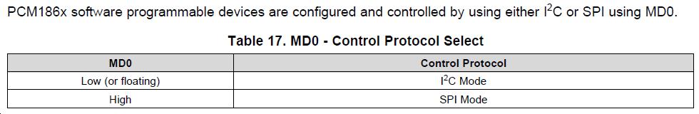

2.1. I2C地址
8bit I2C地址(b100101’AD”R/W’, 0x94 or 0x96)

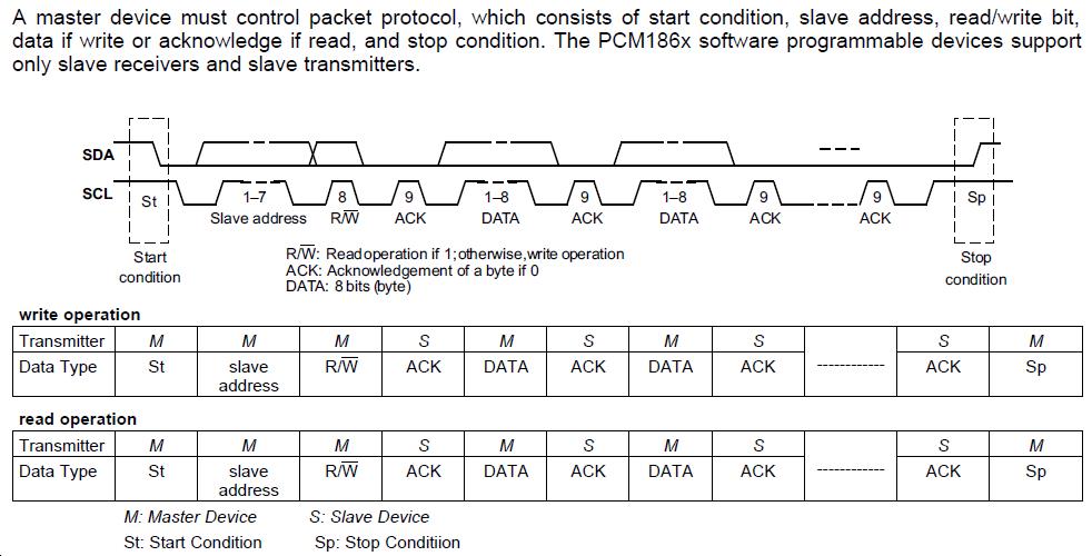
2.2. 通信时序
3. 配置时钟源
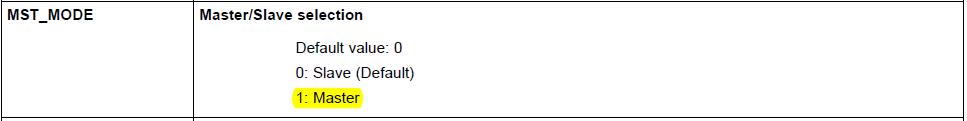
If an external, high quality MCLK is available (either on the SCK pin or XTAL), then the PCM186x should be configured to run in Master Mode where possible, with the ADC and serial ports being driven from the MCLK/SCK source. The on-chip DSPs will continue to require clocks from the PLL, as they run from a much higher clock rate.
Clock MUXs and overall configuration can be done in register Page0, 0x20. For the best performance in master mode, where possible, the automatic clock configuration circuitry will configure the clocks as shown in Table 9, depending on if the device is a PCM186x software programmable device. The tables below show data at 48kHz multiples, the ratios for multiples of 44.1kHz are identical, while the absolute MHz values will be multiples of 44.1kHz instead of 48kHz.
This automatic configuration can be bypassed using registers, starting from CLKDET_EN (Page.0, 0x20).
PCM1863工作在软件可编程模式
3.1. 配置时钟源寄存器0x20
- 设置成主模式
- 选择外部时钟源SCKI

- 默认使能CLKDET_EN,打开自动配置模式,因此不需要配置ADC_CLK_SRC、DSP2_CLK_SRC、DSP1_CLK_SRC
- 配置BCK, LRCK的时钟频率

如上图所示,在master mode时,配置0x26, 0x27寄存器,可以得到想要的BCK和LRCK的速率。查询Table 9,可得知当输入时钟SCK Frequence是24.576MHz时,可用的采样频率有48K,96K,192K,采样频率等于LRCK速率。

- LRCK=96KHz=SCKFrequence/CLKDIVMSTSCK(Reg0x26)/CLKDIVMSTBCK(Reg0x27)
- BCK=6.14M=SCKFrequence/CLKDIVMSTSCK(Reg0x26)
- 将SCK Frequence = 24.576MHz带入上述公式,可得CLK_DIV_MST_SCK = 4,CLK_DIV_MST_BCK=64
3.2. 配置SCK寄存器0x26, 0x27


4. 配置输入和输出
- PCM1863支持最多4路模拟输入+1路双声道I2S输入,支持1路双声道I2S输出
- 双声道I2S输入需要和PM1863共用一组I2S时钟

4.1. 配置首要模拟音频信号输入源
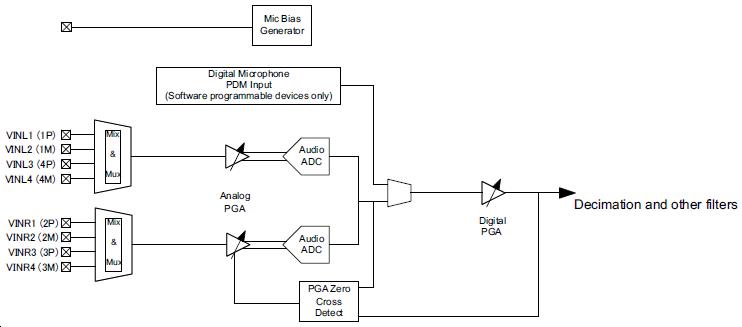
- 本设计使用VINL2和VINR2作为模拟输入源,没有使用模拟麦克风和数字麦克风
- 关闭mic bias,配置寄存器0x15


- 配置寄存器0x06,0x07


4.2. 配置次要模拟信号输入源
The secondary ADC has two main purposes in the PCM186x family. The primary purpose is to act as a low power signal detection system, to aid with system wakeup from sleep. TI calls this functionality “Energysense”.
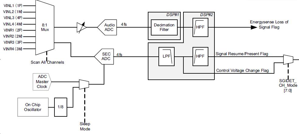
- 改变SGIDET_CH_Mode的值可以在Energysense和Controlsense这两个模式之间切换,默认配置为Energysense
- 次要模拟输入的输入范围是0-1.65V
- 次要模拟输入通道配置为不选择

4.3. 配置I2S信号输入
本设计没有使用I2S输入,可以直接使用寄存器0x08的默认配置:

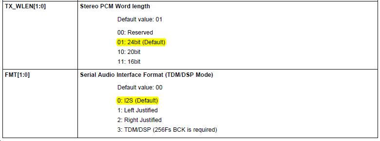
4.4. 配置I2S信号输出
配置I2S格式,寄存器0x08的默认配置:
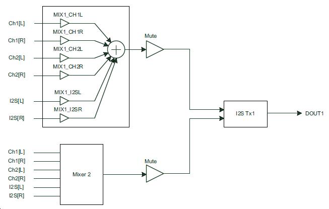
4.5. 配置输出mixer
This function allows post ADC mixing, as well as ADC + incoming I2S mix. Volume control functionality can be performed prior to outputting the signal to an I2S DAC or Amplifier.
Gain range is from –100dB to + 18dB (20 bits negative up +18dB, 4.20 format).
As the DSP coefficients are directly written, no soft ramping is available. Use of I2S receive sacrifices 2 digital mic channels due to pin limitations.
Coefficients are written indirectly to virtual memory addresses using the registers on Page 1.
5. 其他配置
- 配置自动削波抑制:此功能的作用是在检测到削波发生时,自动降低模拟输入的增益,默认是关闭的。
- 模拟音频输入信号强度检测:可以用作睡眠唤醒(最低可检测到的信号强度是-57dBdBFS)。
- 未用作音频输入的模拟输入:可用来检测直流电压的改变,其值可以通过读取I2C寄存器获取。
- GPIO配置:可用作中断输出脚,也可用作一般GPIO脚。
6. 示例代码
const uint8_t IIC_REG_1863[IIC_REG_1863_SIZE][2] =

/* Page 0 Configuration */

    0x00,0x00,    /* Register page selection = page 0 */

    0x05,0x9b,    /* PGA setting:
                    b[7] = 1: Enable mooth change
                    b[6] = 0: Independent  PGA Control
                    b[5] = 0: Disable clipping detection after digital PGA
                    b[4:3] = 1_1: Attenuation limit of the automatic clipping suppression is -6dB
                    b[2:1] = 01: Start automatic clipping supression after clipping is detected 40 time
                    b[0] = 1: Enable automatic clipping suppression */

    0x06,0x42,    /* ADC1L input select
                    b[7] = 0: Not change signal polarity
                    b[6] = Reserved
                    b[5:0] = 0000_10: ADC input channel select VIN2L[SE] */

    0x07,0x42,    /* ADC1R input select
                        b[7] = 0: Not change signal polarity
                        b[6] = Reserved
                        b[5:0] = 0000_10: ADC input channel select VIN2R[SE] */

    0x08,0x40,    /* ADC2L input select
                        b[7] = 0: Not change signal polarity
                        b[6] = Reserved
                        b[5:0] = 0000_00: ADC input channel select none */

    0x10,0x00,    /* GPIO1/2 configuration
                        b[7] = 0: GPIO1 normal polarity
                        b[6:4] = 000: GPIO1
                        b[3] = 0: GPIO0 normal polarity
                        b[2:0] = 000: GPIO0*/

    0x11,0x00,    /* GPIO3/4 configuration
                        b[7] = 0: GPIO3 normal polarity
                        b[6:4] = 000: GPIO3
                        b[3] = 0: GPIO4 normal polarity
                        b[2:0] = 000: GPIO4*/

    0x20,0x11,    /* SCK configuration
                        b[7:6] = 00: SCK/Xtal select SCK or Xtal
                        b[5] = 0: Select SCK
                        b[4] = 1: I2S master mode
                        b[3:1] = 000: ADC/DSP clock source select, ignored if auto clock detector enabled
                        b[0] = 1: Enable auto clock detector */

/* Page 3 Configuration */

    0x00,0x03,    /* Register page selection = page 3 */

    0x15,0x00,    /* Mic control
                        b[4] = 0: Disable mic bias resistor bypass
                        b[0] = 0: Power down mic bias control */

    0x00,0x00,    /* Register page selection = page 0 */
;
以上是关于PCM1863应用笔记的主要内容,如果未能解决你的问题,请参考以下文章