十分钟快速自制CMSIS_DAP仿真器,将ST-LINK-V2变身DAP仿真器!
Posted y-zheng
tags:
篇首语:本文由小常识网(cha138.com)小编为大家整理,主要介绍了十分钟快速自制CMSIS_DAP仿真器,将ST-LINK-V2变身DAP仿真器!相关的知识,希望对你有一定的参考价值。
十分钟快速自制CMSIS_DAP仿真器,将ST-LINK-V2变身DAP仿真器!
(一)简介
说到单片机仿真器(下载器)首先想到的就是J-LINK和ST-LINK,很多人可能还是第一次听说DAP仿真器,那么就先介绍一下。
CMSIS DAP是ARM官方推出的开源仿真器,支持所有的Cortex-A/R/M器件,支持JTAG/SWD接口。有以下特点:
- 完全开源,没有版权限制,所以相应的价格会很便宜
- 不需要安装驱动,即插即用
- 在新版本的DAP里集成了串口,除了下载调试外还能充当USB转串口模块,一机两用
- 性能方面已经可以满足一般用户的需求
市面上基本所有的离线下载器基本都是基于CMSIS_DAP方案来的,例如正点原子的离线下载器、无线下载器等,还有就是国产单片机厂家做的调试器,例如GD32出的GD-LINK,都是基于CMSIS DAP方案改的。
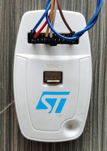
而ST-LINK是ST官方出的,目前有V1、V2、V3版本,并且闭源,正版的很贵!你买到的很便宜,可能也就十几三十几块钱得样子,这是因为这都是盗版的!网上早就有人把ST-LINK-V2的固件给破解出来的,而且原理图也有,所以市面上的便宜货都是根据官方的原理图做出来的板子,然后下载进固件就完成了一个ST-LINK调试器!但是他们是没有ST-LINK的固件源代码的!
什么是在线调试下载?
在线调试器就是用keil或者iar等软件对目标MCU进行调试和下载程序,适用于开发阶段。像是ST-LINK、J-LINK就是在线调试器。
什么是离线下载?
当项目开发中已经接近尾声或者已经成熟后,那么每生产一块板子就需要刷程序,但是刷程序就需要连接到PC机上通过软件刷,这样的话就非常的麻烦,那么有没有一种方式是做一个小板子,把下载程序的功能集成到这个小板子中,这样的话刷程序就是用这个小板子给目标MCU刷程序,就是手持式的。
有!就是离线下载器!
离线下载器的功能说简单点就是Keil下载程序的功能!
关于本篇
教程持续更新,最终的目的是做一个在线调试+离线下载完整功能的仿真器。
本篇教程就先实现用keil能够在线调试下载程序和调试的功能,这是实现完整功能最简单的一步。
(二)调试器的原理
在教程开始之前,我觉得有必要说一下调试器的原理以及他是怎么工作的,怎么把程序下载到目标MCU的,这里以KEIL+ST-LINK为例进行说明。
我们使用keil下载程序的时候,必须要选定一个下载算法,如下所示:
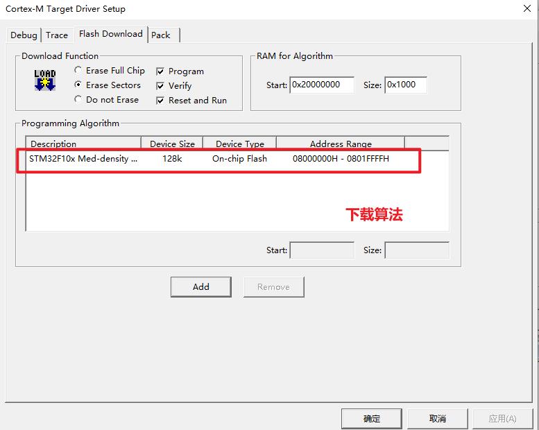
当你使用STM32的时候必须要安装pack包,而下载算法就在pack包内,安装好后就在keil软件的安装目录下了,具体在这里:
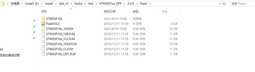
Keil会根据你当前工程使用的芯片,自动去识别应该用哪一个下载算法,例如我目前这个工程是用的STM32F103C8这个芯片,FLASH容量是64K的,属于这个系列的小容量,那么KEIL就自动给我识别了STM32F103x_128.FLM这个下载算法。
那么这个下载算法是什么东西?
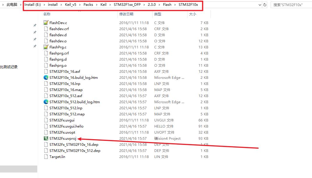
进入这个目录后,他有一个工程,而这个工程就是下载算法的模板工程,我们打开看一下:
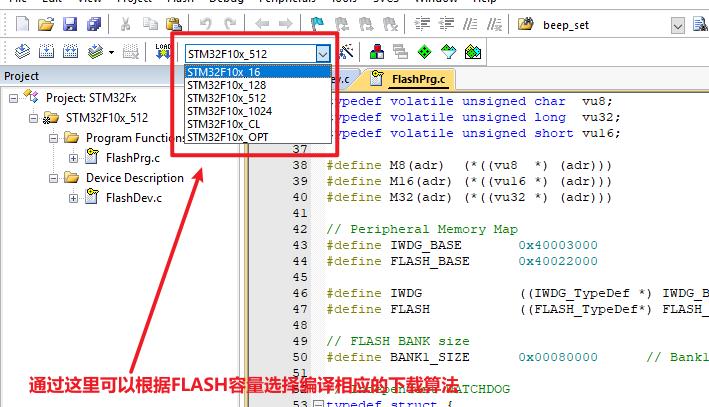
打开工程后很简单的,就只有两个文件,函数也很简单都是对FLASH的操作,编译一下看看:
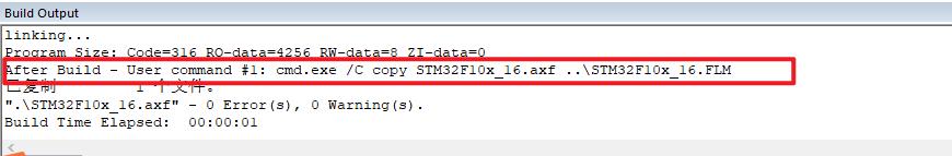
AXF(ARM Executable File)是ARM芯片使用的文件格式,它除了包含bin代码外,还包括了输出给调试器的调试信息
看到没!编译完了之后生成了STM32F103x_16.axf文件,然后只是做了一个文件复制并且重命名成了STM32F10x_16.FLM文件!
现在对下载算法就明确了,下载算法其实就是对目标MCU的FLASH的一系列操作函数!
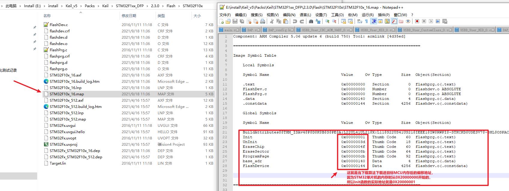
那么KEIL给目标MCU下载程序的时候,其实就是解析出编译好的.axf文件,然后通过USB连接线经过ST-LINK先将下载算法加载进目标MCU的内存中并运行,由于.axf文件中包含的信息很多,其中就有当程序加载进内存后函数在内存中的地址,这个地址也可以通过.map文件查看(.map文件也是keil在编译完工程后生成的),知道函数在内存中的地址,就可以在外部通过特定的进行调用,所以STLINK就是接收来自KEIL的固件程序,然后操控目标单片机内存中的FLASH的操作函数,在通过SWD协议将固件下载进目标MCU的FLASH中,就这样实现了程序下载,后面我们会做离线下载器那么也就明确了,可以将接收KEIL的下发固件这一个步骤变成本地SD卡存储固件,这样不就实现了离线~
现在keil整个下载程序的流程清楚了后,我们的CMSIS_DAP就可以分成两步骤进行:
- 第一步:实现KEIL通过USB和DAP的通信
- 第二步:DAP通过SWD协议将收到固件下载进目标MCU
对于第一步,我们使用STM32CubeMX软件生成工程,然后对源码进行一个简单的修改就可以完成。如果你对USB没有一个充分的了解,本章教程可以先不用管为什么这么修改源代码,跟着步骤来即可,我的另一篇博客有对USB相关知识的扫盲,可以帮助你快速了解:https://blog.csdn.net/qq153471503/article/details/116053851
对于第二步,我们需要移植自ARM官方的CMSIS_DAP源码,源代码在Keil软件的安装目录下,ARM官方的代码是基于LPC单片机的,但是不妨碍我们移植使用:
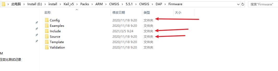
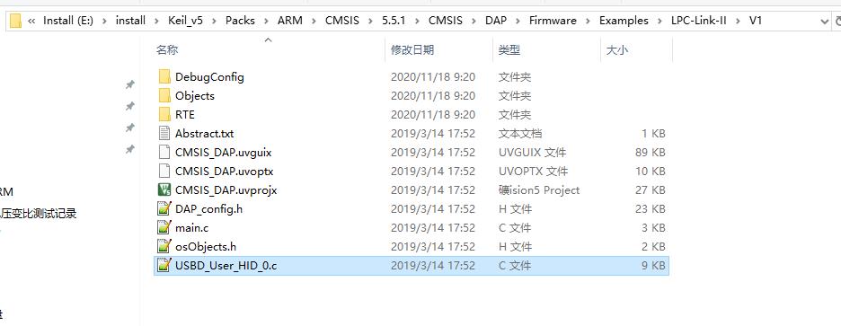
我们需要的就是上图中这三个文件夹中的源文件以及USBD_User_HID_0.c文件即可,这个文件在这里:
(三)工程配置
紧接上文,现在开始实现第一步,由于我目前手头没有现成的硬件,然后我想起ST-LINK其实也是个STM32F103C8单片机,那么我用STLINK的板子不就行了,而且在网上还能找到原理图,省去了自己做板子验证的步骤,等软件调试完毕后,在做板子把它做得小巧精致些。
它的原理图是这样的:
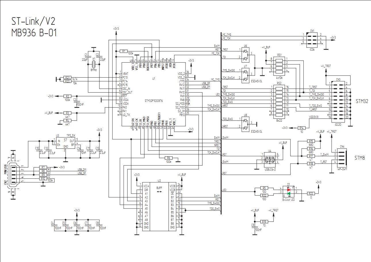
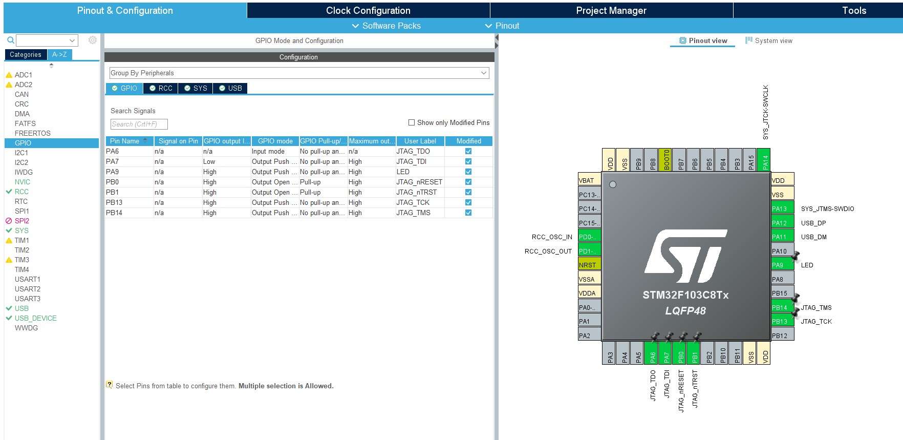
从原理图上可知,使用的引脚分布如下:
- JTAG_nTRST(PB1)
- JTAG_nRESET(PB0)
- JTAG_TDI(PA7)
- JTAG_TMS(PB14,这个引脚也是SWD模式下的SWDIO引脚)
- JTAG_TCK(PB13/PA5,这个引脚也是SWD模式下的SWCLK引脚)
- JTAG_TDO(PA6/PA10)
- LED灯(PA9,低电平为红灯,高电平为绿灯)
对于JTAG_TCK,这是时钟信号引脚,官方用了PB13和PA5两个引脚,我猜测是因为为了提高抗干扰能力,JTAG和SWD两种模式下,使用不同的引脚当做时钟信号。JTAG_TMS引脚同理。
对于JTAG_TDO,当JTAG模式时,这是JTAG的数据输入引脚,当使用SWD模式时,这个引脚可以作为调试输出的作用,所以也是分成了两个引脚来用。
在本教程中,我们就各只用一个IO就可以,不搞那么麻烦。
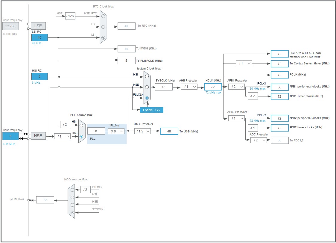
下面开始贴一下我的配置,时钟配置到72M,并开启USB配置成48M,如下:
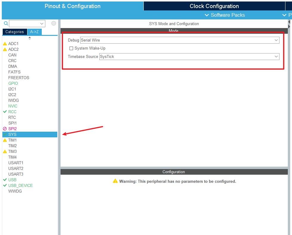
下载程序的调试接口配置为SWD模式:
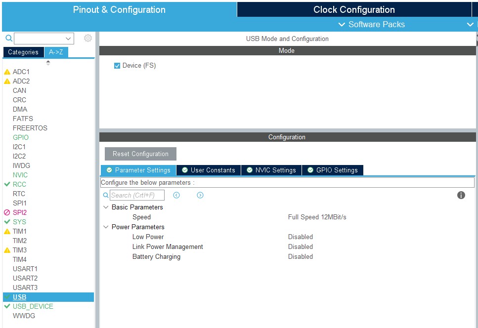
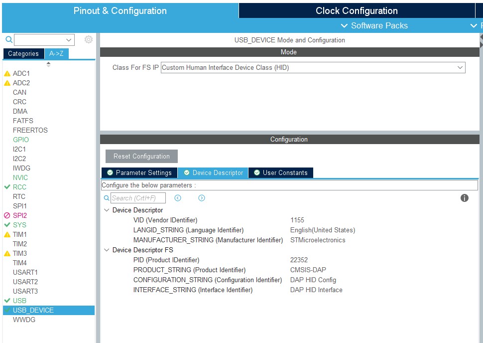
USB的配置如下:
IO引脚的配置如下:
这就是全部的配置内容,然后生成代码就可以了!
(四)移植DAP源码
将DAP加入我们的工程,如下所示:
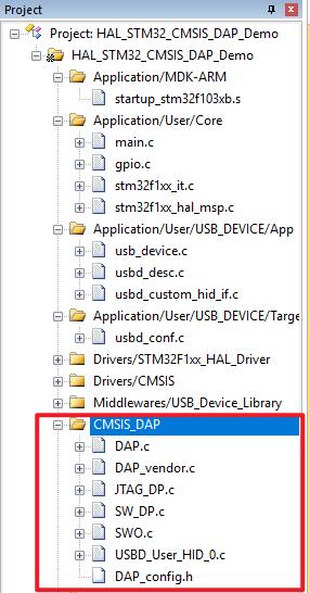
对于DAP源码的移植,我们主要就是修改DAP_config.h和USBD_User_HID_0.c俩文件,其中DAP_config.h是修改的GPIO以及DAP的一些默认配置参数,USBD_User_HID_0.c就是USB与PC的函数接口了,由于原CMSIS_DAP工程是基于LCP单片机并且跑了系统的,而我没有跑系统,所以就需要将USBD_User_HID_0.c文件中使用系统了的API换成轮训方式即可,下面贴一下我的配置:
DAP_config.h文件:
/*
 * Copyright (c) 2013-2017 ARM Limited. All rights reserved.
 *
 * SPDX-License-Identifier: Apache-2.0
 *
 * Licensed under the Apache License, Version 2.0 (the License); you may
 * not use this file except in compliance with the License.
 * You may obtain a copy of the License at
 *
 * www.apache.org/licenses/LICENSE-2.0
 *
 * Unless required by applicable law or agreed to in writing, software
 * distributed under the License is distributed on an AS IS BASIS, WITHOUT
 * WARRANTIES OR CONDITIONS OF ANY KIND, either express or implied.
 * See the License for the specific language governing permissions and
 * limitations under the License.
 *
 * ----------------------------------------------------------------------
 *
 * $Date:        1. December 2017
 * $Revision:    V2.0.0
 *
 * Project:      CMSIS-DAP Configuration
 * Title:        DAP_config.h CMSIS-DAP Configuration File (Template)
 *
 *---------------------------------------------------------------------------*/

#ifndef __DAP_CONFIG_H__
#define __DAP_CONFIG_H__


//**************************************************************************************************
/**
\\defgroup DAP_Config_Debug_gr CMSIS-DAP Debug Unit Information
\\ingroup DAP_ConfigIO_gr
@{
Provides definitions about the hardware and configuration of the Debug Unit.

This information includes:
 - Definition of Cortex-M processor parameters used in CMSIS-DAP Debug Unit.
 - Debug Unit Identification strings (Vendor, Product, Serial Number).
 - Debug Unit communication packet size.
 - Debug Access Port supported modes and settings (JTAG/SWD and SWO).
 - Optional information about a connected Target Device (for Evaluation Boards).
*/

#include "main.h"

/// Processor Clock of the Cortex-M MCU used in the Debug Unit.
/// This value is used to calculate the SWD/JTAG clock speed.
#define CPU_CLOCK               72000000U       ///< Specifies the CPU Clock in Hz.

/// Number of processor cycles for I/O Port write operations.
/// This value is used to calculate the SWD/JTAG clock speed that is generated with I/O
/// Port write operations in the Debug Unit by a Cortex-M MCU. Most Cortex-M processors
/// require 2 processor cycles for a I/O Port Write operation.  If the Debug Unit uses
/// a Cortex-M0+ processor with high-speed peripheral I/O only 1 processor cycle might be
/// required.
#define IO_PORT_WRITE_CYCLES    2U              ///< I/O Cycles: 2=default, 1=Cortex-M0+ fast I/0.

/// Indicate that Serial Wire Debug (SWD) communication mode is available at the Debug Access Port.
/// This information is returned by the command \\ref DAP_Info as part of <b>Capabilities</b>.
#define DAP_SWD                 1               ///< SWD Mode:  1 = available, 0 = not available.

/// Indicate that JTAG communication mode is available at the Debug Port.
/// This information is returned by the command \\ref DAP_Info as part of <b>Capabilities</b>.
#define DAP_JTAG                1               ///< JTAG Mode: 1 = available, 0 = not available.

/// Configure maximum number of JTAG devices on the scan chain connected to the Debug Access Port.
/// This setting impacts the RAM requirements of the Debug Unit. Valid range is 1 .. 255.
#define DAP_JTAG_DEV_CNT        8U              ///< Maximum number of JTAG devices on scan chain.

/// Default communication mode on the Debug Access Port.
/// Used for the command \\ref DAP_Connect when Port Default mode is selected.
#define DAP_DEFAULT_PORT        1U              ///< Default JTAG/SWJ Port Mode: 1 = SWD, 2 = JTAG.

/// Default communication speed on the Debug Access Port for SWD and JTAG mode.
/// Used to initialize the default SWD/JTAG clock frequency.
/// The command \\ref DAP_SWJ_Clock can be used to overwrite this default setting.
#define DAP_DEFAULT_SWJ_CLOCK   10000000U       ///< Default SWD/JTAG clock frequency in Hz.

/// Maximum Package Size for Command and Response data.
/// This configuration settings is used to optimize the communication performance with the
/// debugger and depends on the USB peripheral. Typical vales are 64 for Full-speed USB HID or WinUSB,
/// 1024 for High-speed USB HID and 512 for High-speed USB WinUSB.
#define DAP_PACKET_SIZE         64U             ///< Specifies Packet Size in bytes.

/// Maximum Package Buffers for Command and Response data.
/// This configuration settings is used to optimize the communication performance with the
/// debugger and depends on the USB peripheral. For devices with limited RAM or USB buffer the
/// setting can be reduced (valid range is 1 .. 255).
#define DAP_PACKET_COUNT        8U              ///< Specifies number of packets buffered.

/// Indicate that UART Serial Wire Output (SWO) trace is available.
/// This information is returned by the command \\ref DAP_Info as part of <b>Capabilities</b>.
#define SWO_UART                0               ///< SWO UART:  1 = available, 0 = not available.

/// Maximum SWO UART Baudrate.
#define SWO_UART_MAX_BAUDRATE   10000000U       ///< SWO UART Maximum Baudrate in Hz.

/// Indicate that Manchester Serial Wire Output (SWO) trace is available.
/// This information is returned by the command \\ref DAP_Info as part of <b>Capabilities</b>.
#define SWO_MANCHESTER          0               ///< SWO Manchester:  1 = available, 0 = not available.

/// SWO Trace Buffer Size.
#define SWO_BUFFER_SIZE         4096U           ///< SWO Trace Buffer Size in bytes (must be 2^n).

/// SWO Streaming Trace.
#define SWO_STREAM              0               ///< SWO Streaming Trace: 1 = available, 0 = not available.

/// Clock frequency of the Test Domain Timer. Timer value is returned with \\ref TIMESTAMP_GET.
#define TIMESTAMP_CLOCK         72000000U       ///< Timestamp clock in Hz (0 = timestamps not supported).

/// Debug Unit is connected to fixed Target Device.
/// The Debug Unit may be part of an evaluation board and always connected to a fixed
/// known device.  In this case a Device Vendor and Device Name string is stored which
/// may be used by the debugger or IDE to configure device parameters.
#define TARGET_DEVICE_FIXED     0               ///< Target Device: 1 = known, 0 = unknown;

#if TARGET_DEVICE_FIXED
#define TARGET_DEVICE_VENDOR    "ARM"           ///< String indicating the Silicon Vendor
#define TARGET_DEVICE_NAME      "Cortex-M4"     ///< String indicating the Target Device
#endif

/** Get Vendor ID string.
\\param str Pointer to buffer to store the string.
\\return String length.
*/
__STATIC_INLINE uint8_t DAP_GetVendorString (char *str)
{
    (void)str;
    return (0U);
}

/** Get Product ID string.
\\param str Pointer to buffer to store the string.
\\return String length.
*/
__STATIC_INLINE uint8_t DAP_GetProductString (char *str)
{
    (void)str;
    return (0U);
}

/** Get Serial Number string.
\\param str Pointer to buffer to store the string.
\\return String length.
*/
__STATIC_INLINE uint8_t DAP_GetSerNumString (char *str)
{
    (void)str;
    return (0U);
}

///@}


//**************************************************************************************************
/**
\\defgroup DAP_Config_PortIO_gr CMSIS-DAP Hardware I/O Pin Access
\\ingroup DAP_ConfigIO_gr
@{

Standard I/O Pins of the CMSIS-DAP Hardware Debug Port support standard JTAG mode
and Serial Wire Debug (SWD) mode. In SWD mode only 2 pins are required to implement the debug
interface of a device. The following I/O Pins are provided:

JTAG I/O Pin                 | SWD I/O Pin          | CMSIS-DAP Hardware pin mode
---------------------------- | -------------------- | ---------------------------------------------
TCK: Test Clock              | SWCLK: Clock         | Output Push/Pull
TMS: Test Mode Select        | SWDIO: Data I/O      | Output Push/Pull; Input (for receiving data)
TDI: Test Data Input         |                      | Output Push/Pull
TDO: Test Data Output        |                      | Input
nTRST: Test Reset (optional) |                      | Output Open Drain with pull-up resistor
nRESET: Device Reset         | nRESET: Device Reset | Output Open Drain with pull-up resistor


DAP Hardware I/O Pin Access Functions
-------------------------------------
The various I/O Pins are accessed by functions that implement the Read, Write, Set, or Clear to
these I/O Pins.

For the SWDIO I/O Pin there are additional functions that are called in SWD I/O mode only.
This functions are provided to achieve faster I/O that is possible with some advanced GPIO
peripherals that can independently write/read a single I/O pin without affecting any other pins
of the same I/O port. The following SWDIO I/O Pin functions are provided:
 - \\ref PIN_SWDIO_OUT_ENABLE to enable the output mode from the DAP hardware.
 - \\ref PIN_SWDIO_OUT_DISABLE to enable the input mode to the DAP hardware.
 - \\ref PIN_SWDIO_IN to read from the SWDIO I/O pin with utmost possible speed.
 - \\ref PIN_SWDIO_OUT to write to the SWDIO I/O pin with utmost possible speed.
*/


// Configure DAP I/O pins ------------------------------

/** Setup JTAG I/O pins: TCK, TMS, TDI, TDO, nTRST, and nRESET.
Configures the DAP Hardware I/O pins for JTAG mode:
 - TCK, TMS, TDI, nTRST, nRESET to output mode and set to high level.
 - TDO to input mode.
*/
__STATIC_INLINE void PORT_JTAG_SETUP (void)
{
    GPIO_InitTypeDef GPIO_InitStruct = {0};

	__HAL_RCC_GPIOA_CLK_ENABLE();
	__HAL_RCC_GPIOB_CLK_ENABLE();
    __HAL_RCC_GPIOC_CLK_ENABLE();

    HAL_GPIO_WritePin(LED_GPIO_Port, LED_Pin, GPIO_PIN_SET);

	HAL_GPIO_WritePin(JTAG_TCK_GPIO_Port, JTAG_TCK_Pin, GPIO_PIN_SET);
	HAL_GPIO_WritePin(JTAG_TMS_GPIO_Port, JTAG_TMS_Pin, GPIO_PIN_SET);
	HAL_GPIO_WritePin(JTAG_nRESET_GPIO_Port, JTAG_nRESET_Pin, GPIO_PIN_SET);
	HAL_GPIO_WritePin(JTAG_TDI_GPIO_Port, JTAG_TDI_Pin, GPIO_PIN_SET);
	HAL_GPIO_WritePin(JTAG_TDO_GPIO_Port, JTAG_TDO_Pin, GPIO_PIN_SET);
	HAL_GPIO_WritePin(JTAG_nTRST_GPIO_Port, JTAG_nTRST_Pin, GPIO_PIN_SET);

	// LED
    GPIO_InitStruct.Pin = LED_Pin;
    GPIO_InitStruct.Mode = GPIO_MODE_OUTPUT_PP;
    GPIO_InitStruct.Pull = GPIO_NOPULL;
    GPIO_InitStruct.Speed = GPIO_SPEED_FREQ_HIGH;
    HAL_GPIO_Init(LED_GPIO_Port, &GPIO_InitStruct);

	// TCK
    GPIO_InitStruct.Pin = JTAG_TCK_Pin;
    GPIO_InitStruct.Mode = GPIO_MODE_OUTPUT_PP;
    GPIO_InitStruct.Pull = GPIO_NOPULL;
    GPIO_InitStruct.Speed = GPIO_SPEED_FREQ_HIGH;
    HAL_GPIO_Init(JTAG_TCK_GPIO_Port, &GPIO_InitStruct);

	// TMS
    GPIO_InitStruct.Pin = JTAG_TMS_Pin;
    GPIO_InitStruct.Mode = GPIO_MODE_OUTPUT_PP;
    GPIO_InitStruct.Pull = GPIO_NOPULL;
    GPIO_InitStruct.Speed = GPIO_SPEED_FREQ_HIGH;
    HAL_GPIO_Init(JTAG_TMS_GPIO_Port, &GPIO_InitStruct);

	// TDI
    GPIO_InitStruct.Pin = JTAG_TDI_Pin;
    GPIO_InitStruct.Mode = GPIO_MODE_OUTPUT_PP;
    GPIO_InitStruct.Pull = GPIO_NOPULL;
    GPIO_InitStruct.Speed = GPIO_SPEED_FREQ_HIGH;
    HAL_GPIO_Init(JTAG_TDI_GPIO_Port, &GPIO_InitStruct);

	// nRESET
    GPIO_InitStruct.Pin = JTAG_nRESET_Pin;
    GPIO_InitStruct.Mode = GPIO_MODE_OUTPUT_OD;
    GPIO_InitStruct.Pull = GPIO_PULLUP;
    GPIO_InitStruct.Speed = GPIO_SPEED_FREQ_HIGH;
    HAL_GPIO_Init(JTAG_nRESET_GPIO_Port, &GPIO_InitStruct);

	// nTRST
    GPIO_InitStruct.Pin = JTAG_nTRST_Pin;
    GPIO_InitStruct.Mode = GPIO_MODE_OUTPUT_OD;
    GPIO_InitStruct.Pull = GPIO_PULLUP;
    GPIO_InitStruct.Speed = GPIO_SPEED_FREQ_HIGH;
    HAL_GPIO_Init(JTAG_nTRST_GPIO_Port, &GPIO_InitStruct);

	// TDO
    GPIO_InitStruct.Pin = JTAG_TDO_Pin;
    GPIO_InitStruct.Mode = GPIO_MODE_INPUT;
    GPIO_InitStruct.Pull = GPIO_NOPULL;
    HAL_GPIO_Init(JTAG_TDO_GPIO_Port, &GPIO_InitStruct);
}

/** Setup SWD I/O pins: SWCLK, SWDIO, and nRESET.
Configures the DAP Hardware I/O pins for Serial Wire Debug (SWD) mode:
 - SWCLK, SWDIO, nRESET to output mode and set to default high level.
 - TDI, nTRST to HighZ mode (pins are unused in SWD mode).
*/
__STATIC_INLINE void PORT_SWD_SETUP (void)
{
    GPIO_InitTypeDef GPIO_InitStruct = {0};

	__HAL_RCC_GPIOA_CLK_ENABLE();
	__HAL_RCC_GPIOB_CLK_ENABLE();
    __HAL_RCC_GPIOC_CLK_ENABLE();

    HAL_GPIO_WritePin(LED_GPIO_Port, LED_Pin, GPIO_PIN_SET);

	HAL_GPIO_WritePin(JTAG_TCK_GPIO_Port, JTAG_TCK_Pin, GPIO_PIN_SET);
	HAL_GPIO_WritePin(JTAG_TMS_GPIO_Port, JTAG_TMS_Pin, GPIO_PIN_SET);
	HAL_GPIO_WritePin(JTAG_nRESET_GPIO_Port, JTAG_nRESET_Pin, GPIO_PIN_SET);
	HAL_GPIO_WritePin(JTAG_TDI_GPIO_Port, JTAG_TDI_Pin, GPIO_PIN_SET);
	HAL_GPIO_WritePin(JTAG_TDO_GPIO_Port, JTAG_TDO_Pin, GPIO_PIN_SET);
	HAL_GPIO_WritePin(JTAG_nTRST_GPIO_Port, JTAG_nTRST_Pin, GPIO_PIN_SET);

	// LED
    GPIO_InitStruct.Pin = LED_Pin;
    GPIO_InitStruct.Mode = GPIO_MODE_OUTPUT_PP;
    GPIO_InitStruct.Pull = GPIO_NOPULL;
    GPIO_InitStruct.Speed = GPIO_SPEED_FREQ_HIGH;
    HAL_GPIO_Init(LED_GPIO_Port, &GPIO_InitStruct);

	// TCK
    GPIO_InitStruct.Pin = JTAG_TCK_Pin;
    GPIO_InitStruct.Mode = GPIO_MODE_OUTPUT_PP;
    GPIO_InitStruct.Pull = GPIO_NOPULL;
    GPIO_InitStruct.Speed = GPIO_SPEED_FREQ_HIGH;
    HAL_GPIO_Init(JTAG_TCK_GPIO_Port, &GPIO_InitStruct);

	// TMS
    GPIO_InitStruct.Pin = JTAG_TMS_Pin;
    GPIO_InitStruct.Mode = GPIO_MODE_OUTPUT_PP;
    GPIO_InitStruct.Pull = GPIO_NOPULL;
    GPIO_InitStruct.Speed = GPIO_SPEED_FREQ_HIGH;
    HAL_GPIO_Init(JTAG_TMS_GPIO_Port, &GPIO_InitStruct);

	// nRESET
    GPIO_InitStruct.Pin = JTAG_nRESET_Pin;
    GPIO_InitStruct.Mode = GPIO_MODE_OUTPUT_OD;
    GPIO_InitStruct.Pull = GPIO_PULLUP;
    GPIO_InitStruct.Speed = GPIO_SPEED_FREQ_HIGH;
    HAL_GPIO_Init(JTAG_nRESET_GPIO_Port, &GPIO_InitStruct);

	// TDI TDO nTRST
	HAL_GPIO_DeInit(JTAG_TDI_GPIO_Port, JTAG_TDI_Pin);
	HAL_GPIO_DeInit(JTAG_TDO_GPIO_Port, JTAG_TDO_Pin);
	HAL_GPIO_DeInit(JTAG_nTRST_GPIO_Port, JTAG_nTRST_Pin);
}

/** Disable JTAG/SWD I/O Pins.
Disables the DAP Hardware I/O pins which configures:
 - TCK/SWCLK, TMS/SWDIO, TDI, TDO, nTRST, nRESET to High-Z mode.
*/
__STATIC_INLINE void PORT_OFF (void)
{
	HAL_GPIO_DeInit(JTAG_TCK_GPIO_Port, JTAG_TCK_Pin);
	HAL_GPIO_DeInit(JTAG_TMS_GPIO_Port, JTAG_TMS_Pin);
	HAL_GPIO_DeInit(JTAG_nRESET_GPIO_Port, JTAG_nRESET_Pin);
	HAL_GPIO_DeInit(JTAG_TDI_GPIO_Port, JTAG_TDI_Pin);
	HAL_GPIO_DeInit(JTAG_TDO_GPIO_Port, JTAG_TDO_Pin);
	HAL_GPIO_DeInit(JTAG_nTRST_GPIO_Port, JTAG_nTRST_Pin);
}


// SWCLK/TCK I/O pin -------------------------------------

/** SWCLK/TCK I/O pin: Get Input.
\\return Current status of the SWCLK/TCK DAP hardware I/O pin.
*/
__STATIC_FORCEINLINE uint32_t PIN_SWCLK_TCK_IN (void)
{
    return JTAG_TCK_GPIO_Port->ODR & JTAG_TCK_Pin ? 1 : 0;
}

/** SWCLK/TCK I/O pin: Set Output to High.
Set the SWCLK/TCK DAP hardware I/O pin to high level.
*/
__STATIC_FORCEINLINE void PIN_SWCLK_TCK_SET (void)
{
    JTAG_TCK_GPIO_Port->BSRR = JTAG_TCK_Pin;
}

/** SWCLK/TCK I/O pin: Set Output to Low.
Set the SWCLK/TCK DAP hardware I/O pin to low level.
*/
__STATIC_FORCEINLINE void PIN_SWCLK_TCK_CLR (void)
{
    JTAG_TCK_GPIO_Port->BRR = JTAG_TCK_Pin;
}


// SWDIO/TMS Pin I/O --------------------------------------

/** SWDIO/TMS I/O pin: Get Input.
\\return Current status of the SWDIO/TMS DAP hardware I/O pin.
*/
__STATIC_FORCEINLINE uint32_t PIN_SWDIO_TMS_IN (void)
{
    return JTAG_TMS_GPIO_Port->ODR & JTAG_TMS_Pin ? 1 : 0;
}

/** SWDIO/TMS I/O pin: Set Output to High.
Set the SWDIO/TMS DAP hardware I/O pin to high level.
*/
__STATIC_FORCEINLINE void PIN_SWDIO_TMS_SET (void)
{
    JTAG_TMS_GPIO_Port->BSRR = JTAG_TMS_Pin;
}

/** SWDIO/TMS I/O pin: Set Output to Low.
Set the SWDIO/TMS DAP hardware I/O pin to low level.
*/
__STATIC_FORCEINLINE void PIN_SWDIO_TMS_CLR (void)
{
    JTAG_TMS_GPIO_Port->BRR = JTAG_TMS_Pin;
}

/** SWDIO I/O pin: Get Input (used in SWD mode only).
\\return Current status of the SWDIO DAP hardware I/O pin.
*/
__STATIC_FORCEINLINE uint32_t PIN_SWDIO_IN (void)
{
    return JTAG_TMS_GPIO_Port->IDR & JTAG_TMS_Pin ? 1 : 0;
}

/** SWDIO I/O pin: Set Output (used in SWD mode only).
\\param bit Output value for the SWDIO DAP hardware I/O pin.
*/
__STATIC_FORCEINLINE void PIN_SWDIO_OUT (uint32_t bit)
{
    if(bit & 0X01)
    {
        JTAG_TMS_GPIO_Port->BSRR = JTAG_TMS_Pin;
    }
    else
    {
        JTAG_TMS_GPIO_Port->BRR = JTAG_TMS_Pin;
    }
}

/** SWDIO I/O pin: Switch to Output mode (used in SWD mode only).
Configure the SWDIO DAP hardware I/O pin to output mode. This function is
called prior \\ref PIN_SWDIO_OUT function calls.
*/
__STATIC_FORCEINLINE void PIN_SWDIO_OUT_ENABLE (void)
{
    GPIO_InitTypeDef GPIO_InitStruct = {0};
    GPIO_InitStruct.Pin = JTAG_TMS_Pin;
    GPIO_InitStruct.Mode = GPIO_MODE_OUTPUT_PP;
    GPIO_InitStruct.Pull = GPIO_NOPULL;
    GPIO_InitStruct.Speed = GPIO_SPEED_FREQ_HIGH;
    HAL_GPIO_Init(JTAG_TMS_GPIO_Port, &GPIO_InitStruct);
}

/** SWDIO I/O pin: Switch to Input mode (used in SWD mode only).
Configure the SWDIO DAP hardware I/O pin to input mode. This function is
called prior \\ref PIN_SWDIO_IN function calls.
*/
__STATIC_FORCEINLINE void PIN_SWDIO_OUT_DISABLE (void)
{
    GPIO_InitTypeDef GPIO_InitStruct = {0};
    GPIO_InitStruct.Pin = JTAG_TMS_Pin;
    GPIO_InitStruct.Mode = GPIO_MODE_INPUT;
    GPIO_InitStruct.Pull = GPIO_NOPULL;
    GPIO_InitStruct.Speed = GPIO_SPEED_FREQ_HIGH;
    HAL_GPIO_Init(JTAG_TMS_GPIO_Port, &GPIO_InitStruct);
}


// TDI Pin I/O ---------------------------------------------

/** TDI I/O pin: Get Input.
\\return Current status of the TDI DAP hardware I/O pin.
*/
__STATIC_FORCEINLINE uint32_t PIN_TDI_IN (void)
{
    return JTAG_TDI_GPIO_Port->ODR & JTAG_TDI_Pin ? 1 : 0;
}

/** TDI I/O pin: Set Output.
\\param bit Output value for the TDI DAP hardware I/O pin.
*/
__STATIC_FORCEINLINE void PIN_TDI_OUT (uint32_t bit)
{
    if(bit & 0X01)
    {
        JTAG_TDI_GPIO_Port->BSRR = JTAG_TDI_Pin;
    }
    else
    {
        JTAG_TDI_GPIO_Port->BRR = JTAG_TDI_Pin;
    }
}


// TDO Pin I/O ---------------------------------------------

/** TDO I/O pin: Get Input.
\\return Current status of the TDO DAP hardware I/O pin.
*/
__STATIC_FORCEINLINE uint32_t PIN_TDO_IN (void)
{
    return JTAG_TDO_GPIO_Port->IDR & JTAG_TDO_Pin ? 1 : 0<以上是关于十分钟快速自制CMSIS_DAP仿真器,将ST-LINK-V2变身DAP仿真器!的主要内容,如果未能解决你的问题,请参考以下文章